
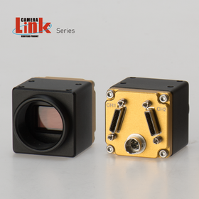
CameraLink Area Camera Series for Semiconductor Manufacturing
Support for defect detection in semiconductor manufacturing with high-reliability CameraLink.
In the semiconductor manufacturing industry, as miniaturization and high integration progress, there is a demand for accurately detecting minute defects to ensure product quality. In particular, with the acceleration of manufacturing lines, high-resolution and high-frame-rate image acquisition has become essential. To avoid overlooking even slight defects and prevent the outflow of defective products, a reliable image inspection system is crucial. The CameraLink area scan camera series achieves high image quality, high sensitivity, and high fps by combining a simple and highly reliable CameraLink interface with SONY Pregius 2nd Gen CMOS sensors, meeting the precise defect detection needs in semiconductor manufacturing. 【Application Scenarios】 - Wafer inspection - Chip appearance inspection - Printed circuit board inspection 【Benefits of Implementation】 - Improved detection accuracy of minute defects - Accelerated inspection processes - Enhanced production yield
- Company:Japan Bopixel Co., Ltd.
- Price:Other
